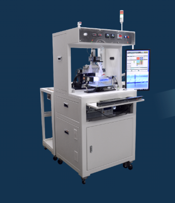
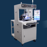
AMEBA 3D S Series
(In stock)
| Product Name | AMEBA 3D S Series |
| Model Number | S-Series models; placeholder — e.g. S-100, S-200) |
| Brand | AMEBA 3D (AnyCasting Co., Ltd.) |
| Category | 3D Circuit / Additive Manufacturing Equipment |
| Country Origin | South Korea |
| Material | Conductive metals / plating metals (Cu, Ag, Ni, Au, Pt, Sn, etc.) in ionic form (via S-ECAM process). |
| Applications | High-resolution 3D circuits, bumps, bonding layers in semiconductors and electronics .Thick and multi-level circuit patterns on substrates (wafer bump, power modules, chip interconnects). |
The AMEBA 3D S Series, leveraging S-ECAM (Selective ElectroChemical Additive Manufacturing), enables the direct 3D printing of complex electronic circuits with high precision and freedom. It supports line widths from 1 µm to 5,000 µm, and line thicknesses from 1 µm to 1,000 µm, enabling high aspect ratios (≥ 1:5) and fine line/space resolutions (e.g. 20 µm or less)
Because the process prints in the state of metal ions, the resulting conductivity approaches that of the pure metal (e.g., for copper, ~5.96 × 10⁷ S/m)
Multiple metals are printable, including Cu, Ni, Ag, Au, Pt, Sn, etc.
Compared with subtractive or etching-based methods (e.g. wet etching or plating), S-ECAM significantly reduces processing steps, eliminates many masking steps, and cuts cost and time. The total processing amount and time are “less than half” compared to conventional multi-step processes.
The S Series is well-suited for applications such as wafer bumping, multi-layer circuits, bond layers in high-power modules, where 3D thickness control and structural freedom are needed. Because AMEBA can print diverse thicknesses and patterns, it offers design flexibility beyond conventional planar processes.
Looks like there are no reviews yet.