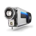
Bruker eWARP
(In stock)
| Product Name | Bruker eWARP |
| Model Number | eWARP |
| Brand | Bruker |
| Category | EBSD Detector / Electron Backscatter Diffraction Detector / Materials Characterization Instrument |
| Country Origin | Germany |
| Material | Direct electron detection sensor (hybrid-pixel CMOS / Wide Area Pixelated (WARP) sensor) Silicon sensor optimized for SEM electron energies /On-chip binning capability allowing high speed and signal efficiency. |
| Applications | High-speed EBSD mapping under low‐to‐medium beam conditions (e.g. 10 kV accelerating voltage, 12 nA beam current) /Large area mapping, 3D EBSD, in-situ / time resolved EBSD during heating or mechanical testing . Materials with fine microstructure, heavily deformed metals / alloys, beam sensitive or insulating materials (due to lower required beam dose) |
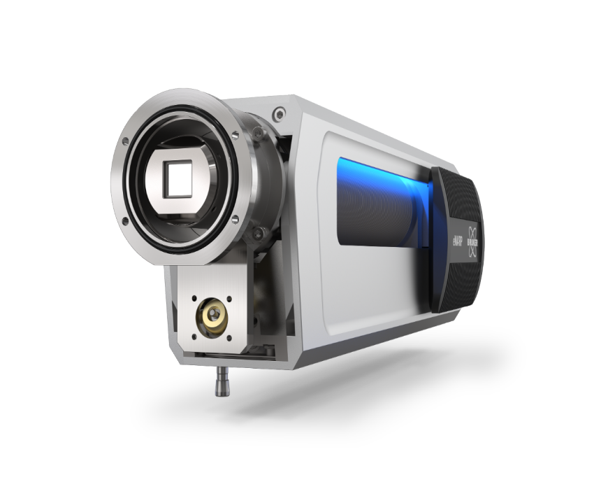
eWARP is the pioneering EBSD detector that works via electrons only. Powered by a revolutionary Bruker-designed camera that combines direct electron detection and CMOS technologies, eWARP delivers unmatched performance and elevates the technique of EBSD to a new level.
eWARP is by far the fastest and most signal efficient EBSD detector in the market. The detector can acquire EBSD maps at a speed of up to 14,400 patterns/second requiring only low-to-medium electron beam conditions, e.g., an accelerating voltage of 10 kV and a probe current of 12 nA.
eWARP’s unprecedented signal efficiency stems from its unique high collection rate, provided by the wide area pixels, and its high conversion rate generated by the silicon sensor designed for SEM electron energies.
eWARP is the revolutionary core of our QUANTAX EBSD system.
Looks like there are no reviews yet.